

The first attempt to automate the manufacture of diffused silicon transistors and pioneering work by Gordon Moore happened at the Silicon Valley location
For tech history buffs, 391 San Antonio Road in Mountain View, Calif., is a well-known address. The site was the home of Shockley Semiconductor Laboratory [above], which played a pivotal role in launching Silicon Valley’s electronics industry. IEEE Fellow William B. Shockley, a Nobel Prize–winning physicist, opened the research lab in 1956.
Many of the chip industry’s founding fathers were researchers there. One was IEEE Life Fellow Gordon Moore, cofounder of Fairchild Semiconductor and Intel. Moore’s Law was named after him. He predicted in 1965 that the transistor density of ICs would double every year for the next decade. The pattern of periodic doublings in density has held for more than 50 years. Moore left Shockley’s lab in 1957 to cofound Fairchild, also in Mountain View, but it was at Shockley where he learned how to produce transistors for commercial sale.
It’s estimated that more than 400 electronics firms can trace their roots to the lab. The IEEE history committee honored the location on 15 August with two IEEE Milestones. One recognizes the impact the laboratory had on the electronics industry; the other notes the work Moore did there.
HOW THE LAB GOT ITS START
After World War II, Mervin Kelly, an executive vice president at Bell Labs, formed a group to research solid-state physics in the hope of producing a replacement for the vacuum tube from semiconducting materials (see The Institute article “Honoring the Trailblazing Transistor”). Led by Shockley and chemist Stanley Morgan, the team included physicists Walter Brattain and John Bardeen, who developed the first transistor in 1947.
In 1951 Shockley built an alternate geometry—the junction transistor, which quickly became the predominant type. The first pocket transistor radios had junction transistors, as did the bombers and intercontinental ballistic missiles of the early Cold War. The November 1952 issue of Proceedings of the Institute of Radio Engineers (now Proceedings of the IEEE) contains Shockley’s article outlining the invention: “Transistor Electronics: Imperfections, Unipolar and Analog Transistors.”
Bardeen, Brattain, and Shockley received the 1956 Nobel Prize in physics for their research on semiconductors and their discovery of the transistor effect. And Shockley was the 1980 IEEE Medal of Honor recipient, “for the invention of the junction transistor, the analog and the junction field-effect transistor, and the theory underlying their operation.”
Shockley left Bell Labs in June 1955. In July he called chemist and industrialist Arnold O. Beckman, who had held a gala in February honoring Shockley and vacuum-tube pioneer Lee de Forest. Beckman and Shockley initially discussed Shockley’s patent for a robotic eye and the possibilities for automating factories.
Shockley approached Beckman again in August, this time to discuss his desire to start a company to bring the new “diffused” silicon transistors to market. Diffusion was substantially more controllable and could yield much narrower base layers, just micrometers thick, and hence transistors that work at higher frequencies. What’s more, he told Beckman, he would develop an automated way to mass-produce the transistors, according to “How William Shockley’s Robot Dream Helped Launch Silicon Valley,” published in IEEE Spectrum.
Beckman and Shockley signed an agreement in September to establish Shockley Semiconductor Lab. It stipulated that the facility would be part of Beckman Instruments for two years. During that time Shockley would have the freedom to pursue new inventions in electronics, according to the article, but the lab’s main priority would be the automated manufacturing of diffused silicon transistors. Although Beckman’s company was headquartered in Southern California, Shockley persuaded him to locate the lab near Palo Alto, where Shockley had grown up. Nearby were electron-tube production plants for military and commercial markets, and San Francisco was just to the north.
Shockley drafted a news release to announce his new laboratory, according to the Spectrum article. “The opportunity to contribute to the growth of a new electronics community will attract men of imagination and initiative along both social and technological lines,” he wrote. “I hope to create a vehicle in which such men can make their maximum contributions and find their greatest satisfactions and rewards.”
GETTING MOORE
One of those Shockley attracted was Moore, who had earned a Ph.D. in chemistry with a minor in physics in 1954 from Caltech. He also held a bachelor’s degree in chemistry from the University of California, Berkeley.
“What he [Shockley] wanted to do really struck my fancy,” Moore said in a 2009 interview with IEEE.tv about his career. “He was after making a very practical device, a silicon transistor, and it looked like it could use some of the skills I had developed as a chemist. I knew absolutely nothing about semiconductors or electronics in general, but that wasn’t a requirement at that time. There were many other things that still had to be solved where my background did fit.”
By most accounts, Shockley was a poor manager. He decided to abandon the diffused silicon transistor in favor of an invention of his own: the four-layer diode. Several researchers, including Moore, were concerned about that project, and by October 1957 he and seven others quit to launch Fairchild. The “traitorous eight,” which is what Shockley called them, focused on making the diffused silicon transistor. Moore perfected the production of silicon planar epitaxial transistors, which became the primary process for manufacturing silicon ICs.
In 1968 Moore went on to cofound Intel, which became the world’s largest semiconductor and memory technology company. In 1975 he became its president and chief executive officer. He was president until 1979 and remained CEO until 1987. He now is chairman emeritus.
He received the 2008 IEEE Medal of Honor “for pioneering technical roles in integrated-circuit processing, and leadership in the development of MOS memory, the microprocessor computer, and the semiconductor industry.” IEEE Spectrum published a special report in 2015 celebrating 50 years of Moore’s Law.
INAUSPICIOUS ENDING
The future of the Shockley Semiconductor Laboratory wasn’t as bright as Fairchild’s, Intel’s, or hundreds of other Silicon Valley companies. The lab never mass-produced a silicon transistor, and it found few takers for the four-layer diode.
Beckman sold the operation in 1960, and it closed several years later. WeWork, which provides shared workspaces, now occupies the site.
Shockley became a professor of electrical engineering at Stanford. He died in 1989.

MILESTONE CEREMONY
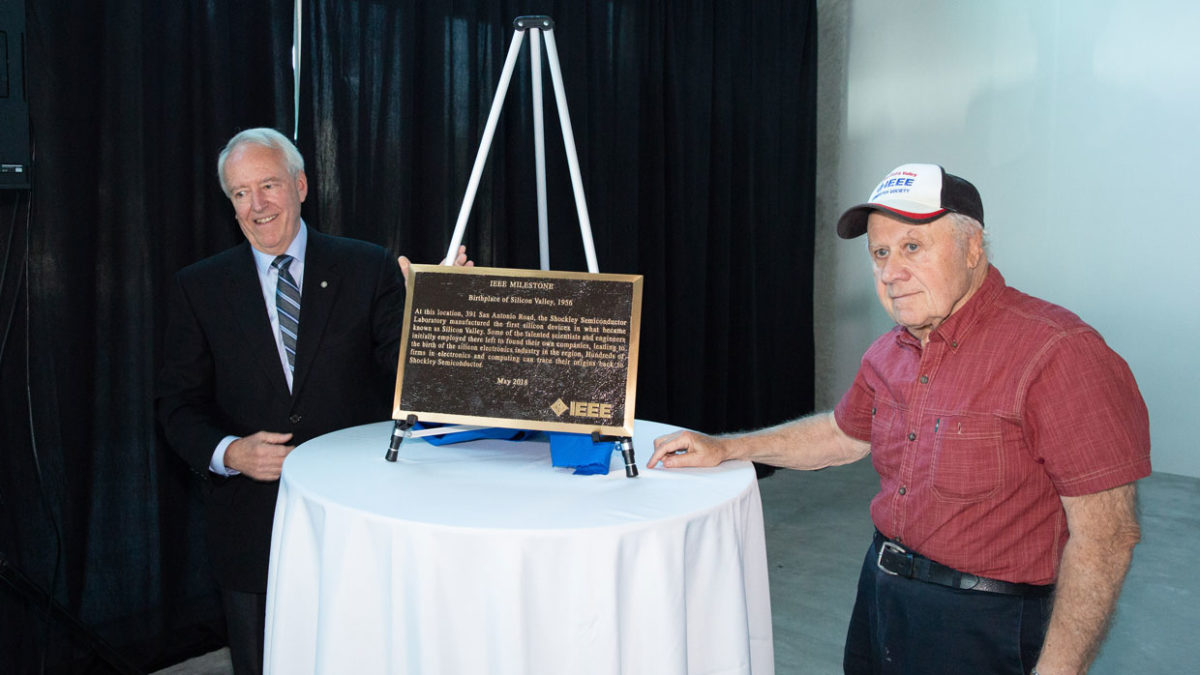
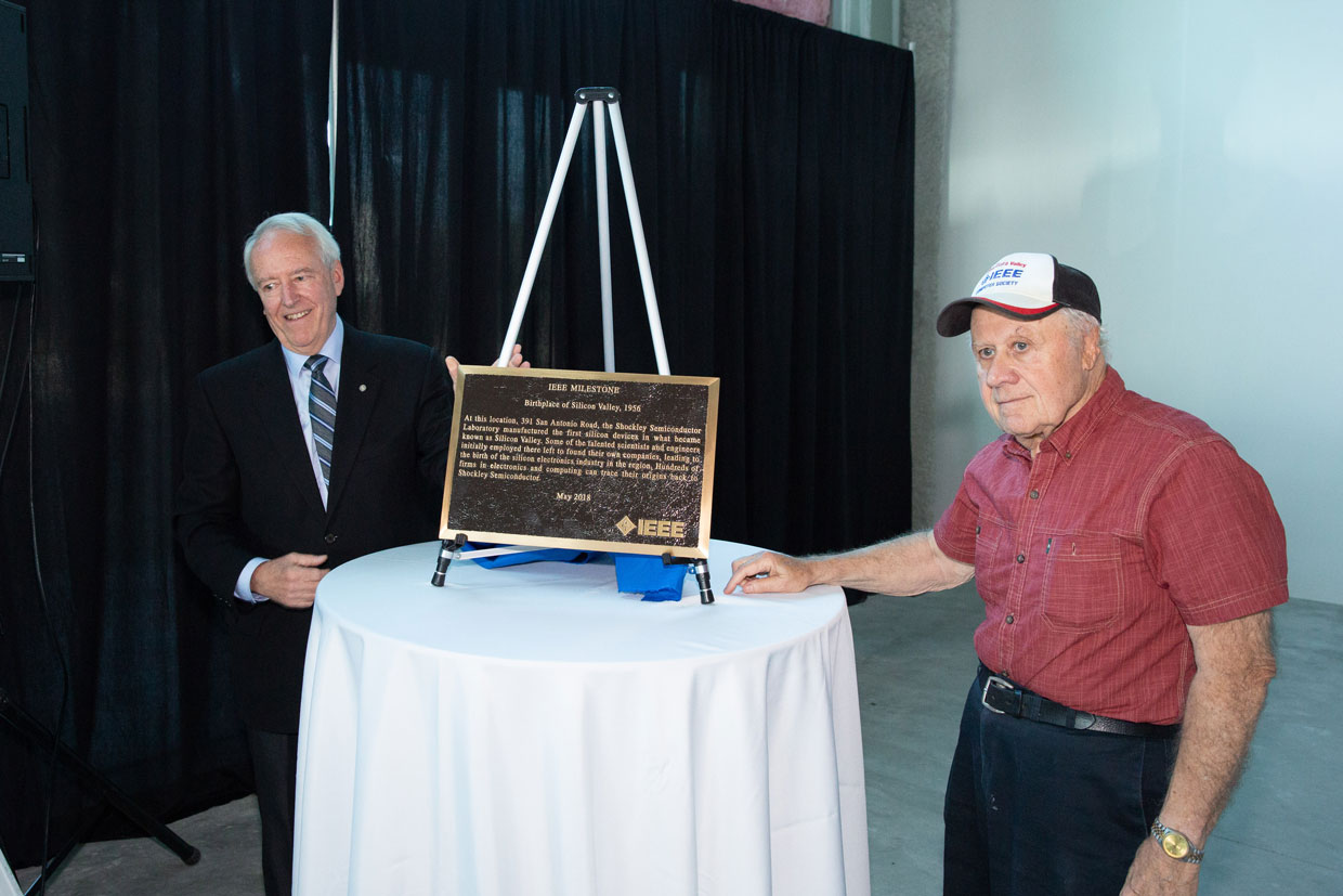
On 15 August two IEEE Milestone plaques were unveiled by the IEEE Santa Clara Valley (California) Section. More than 300 guests attended the ceremony, including several of IEEE’s top leaders.
IEEE President Jim Jefferies unveiled the “Birthplace of Silicon Valley, 1956” plaque, which is mounted on an exterior wall of the WeWork building overlooking San Antonio Road.
It reads, “At this location, 391 San Antonio Road, the Shockley Semiconductor Laboratory manufactured the first silicon devices in what became known as Silicon Valley. Some of the talented scientists and engineers initially employed there left to found their own companies, leading to the birth of the silicon electronics industry in the region. Hundreds of firms in electronics and computing can trace their origins back to Shockley Semiconductor.”
The “Moore’s Law, 1965” plaque was unveiled by 2017 IEEE President Karen Bartleson. It will be located in the site’s technology plaza, adjacent to a video information booth and a piece of artwork in the form of a silicon crystal lattice.
It reads, “Gordon E. Moore, cofounder of Fairchild and Intel, began his work in silicon microelectronics at Shockley Semiconductor Laboratory in 1956. His 1965 prediction at Fairchild Semiconductor, subsequently known as ‘Moore’s Law,’ that the number of components on an integrated circuit will increase exponentially with time while cost per function decreases, guided the industry’s contributions to advances in electronics and computing for more than 50 years.”
This article was written with assistance from the IEEE History Center, which is partially funded by donations to the IEEE Foundation. The Foundation held a reception in conjunction with the dedications of the Milestones to introduce members to “Realize the Full Potential of IEEE” campaign. It seeks to raise US$30 million in support of Foundation-funded programming, such as the IEEE History Center. To date the campaign has succeeded in raising more than $16 million.
Social Media